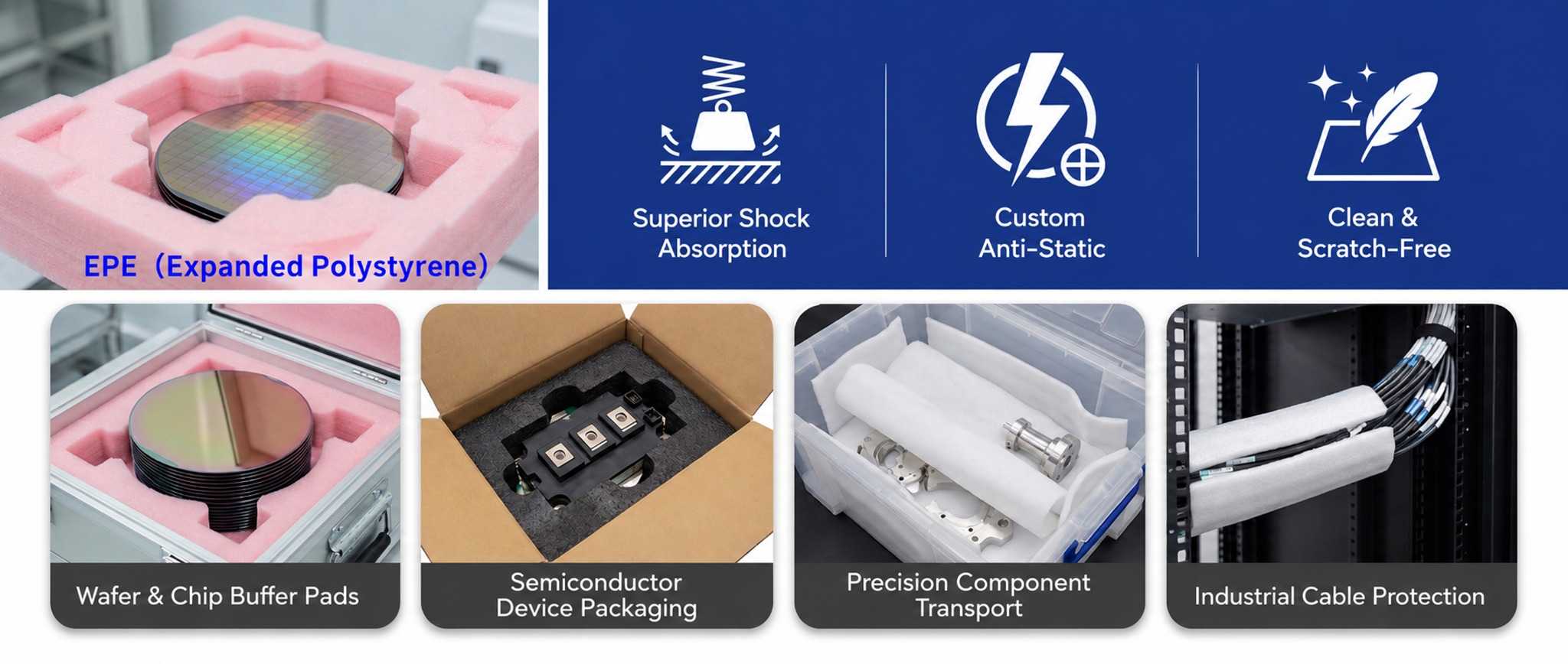
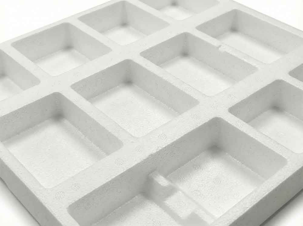
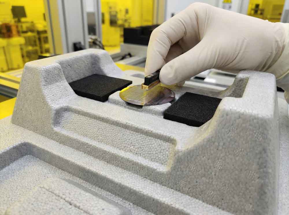
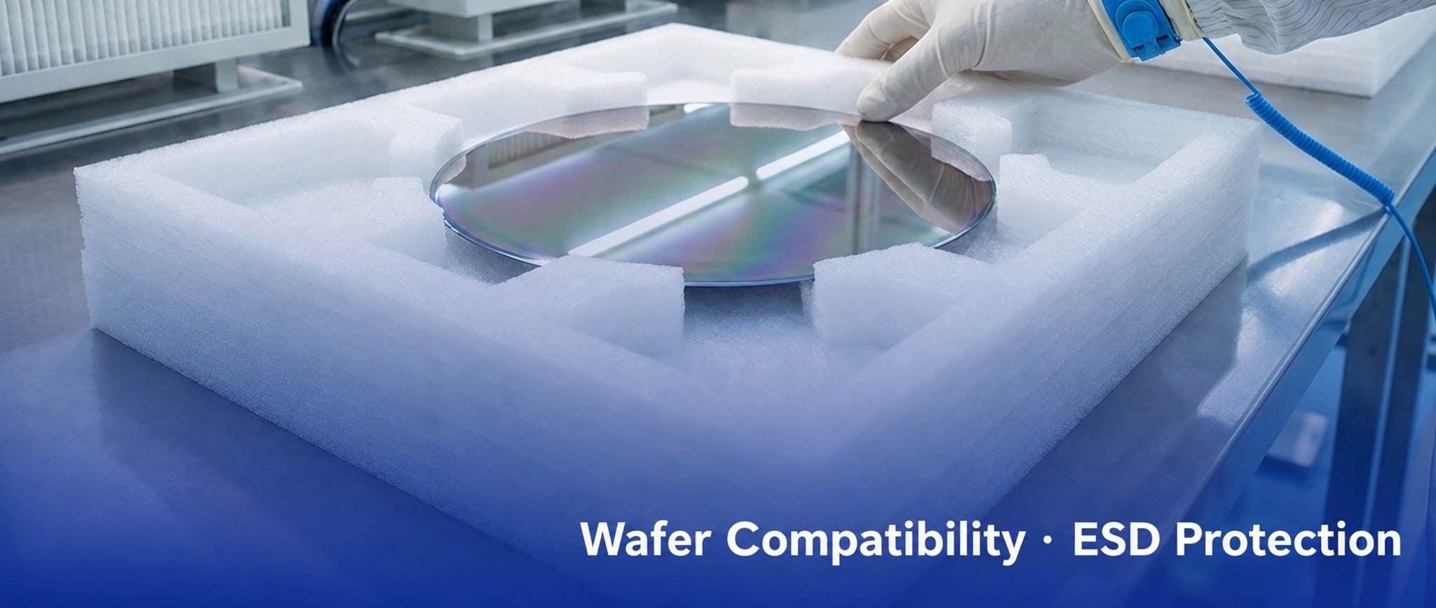
a. Challenge: Wafer sensitivity to vibration, scratching, and electrostatic discharge affecting yield
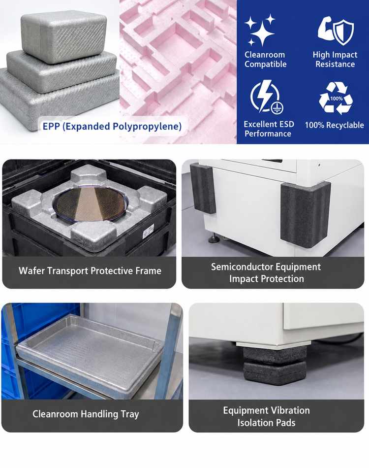
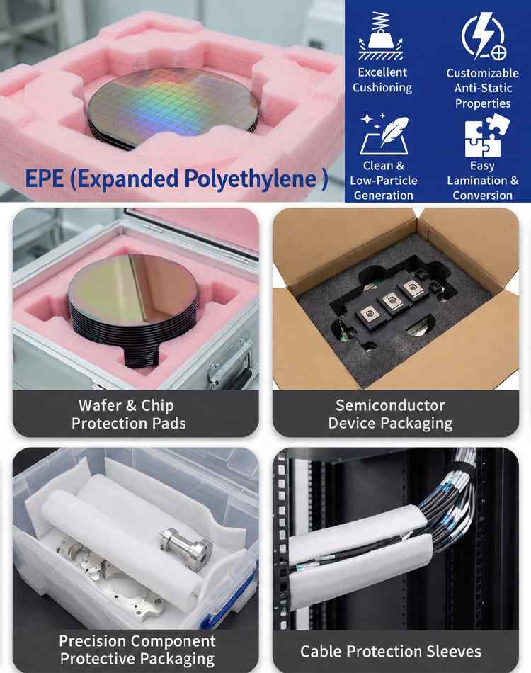
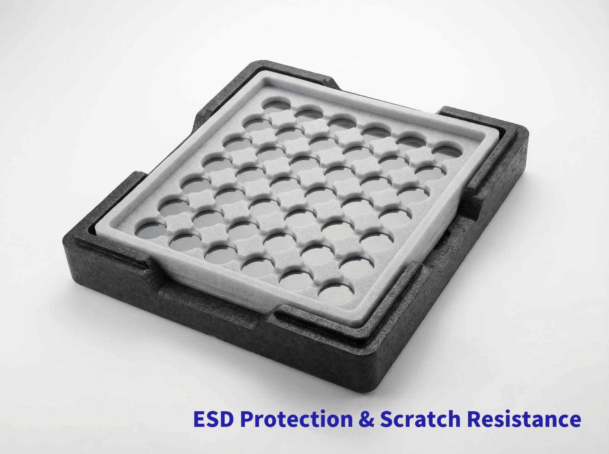
b. Material Selection: Anti-static EPE inner tray + EPP fixing frame
c. Core Benefits: Custom slots for mainstream wafer sizes; rapid electrostatic dissipation; no displacement under drop impact; clean and dust-free environment; significantly improved yield
d. Applications: Long-distance wafer transport boxes, cleanroom transfer containers, and lithography wafer buffering components
e. Image: EPE wafer tray with EPP fixing frame
Chip & Component Packaging
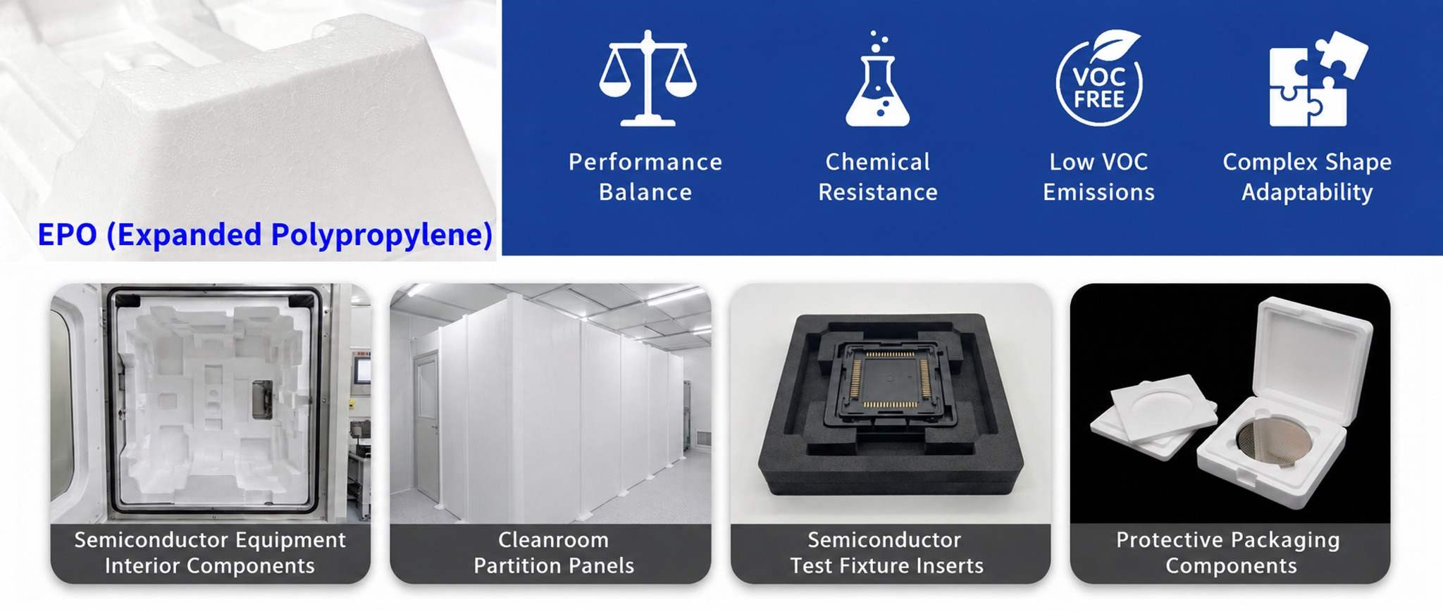
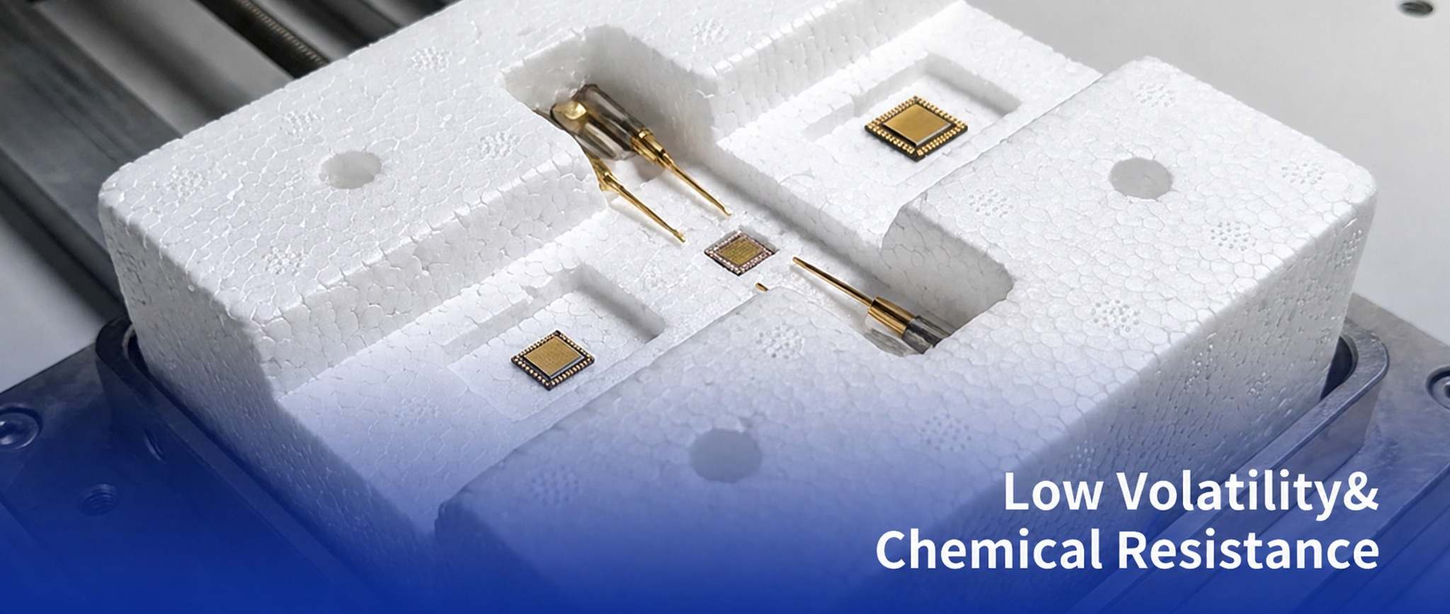
a. Challenge: Moisture, scratching, and chemical contamination during storage and transport
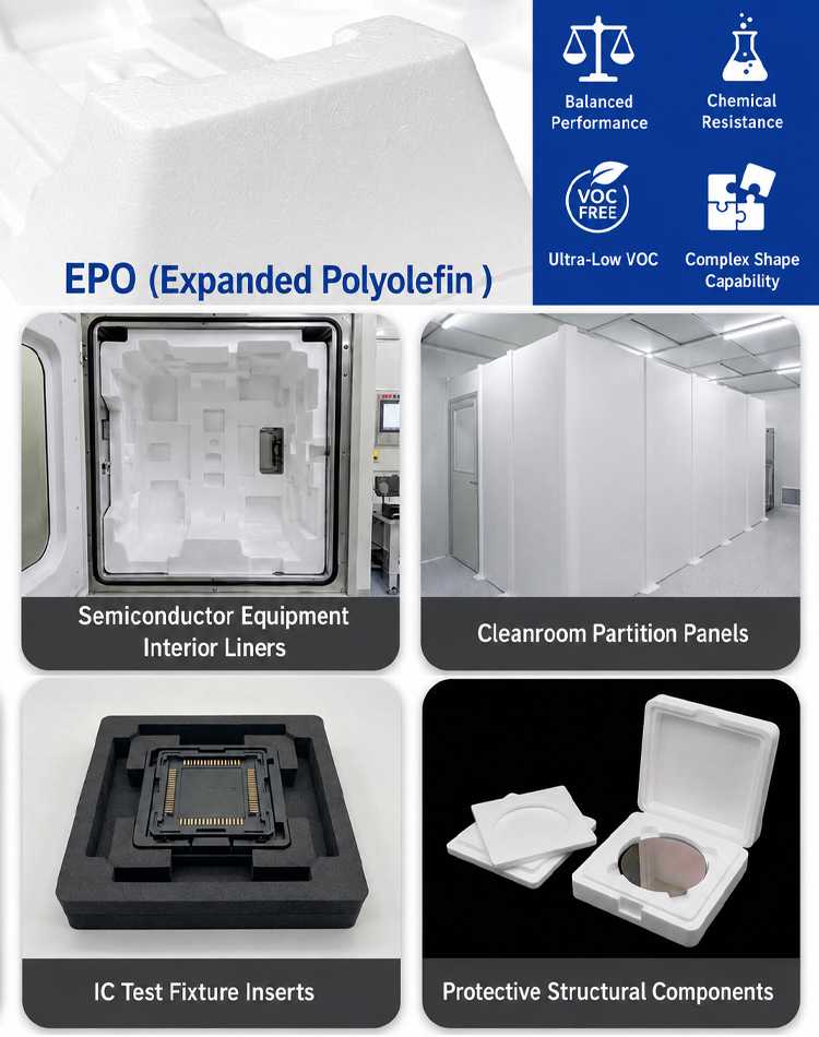
b. Material Selection: Anti-static EPE composite film + EPO custom inserts
c. Core Benefits: Moisture and scratch protection; chemical resistance; no volatile contamination; suitable for long-term storage
d. Applications: Finished chip packaging, semiconductor sensor transport, and precision IC protection
e. Image: EPO custom chip packaging insert
1.Wafer & Chip Packaging & Transportation
Equipment Body & Structural Protection
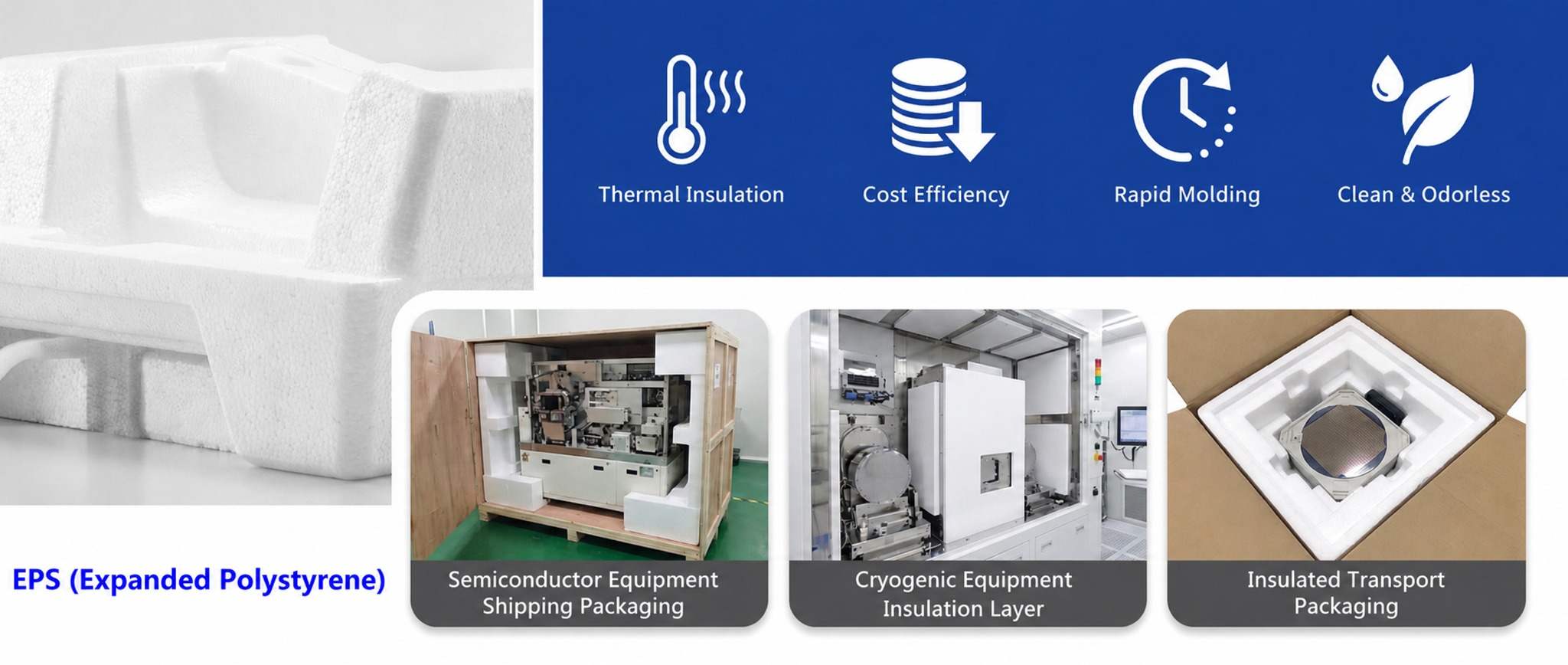
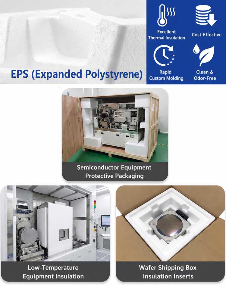
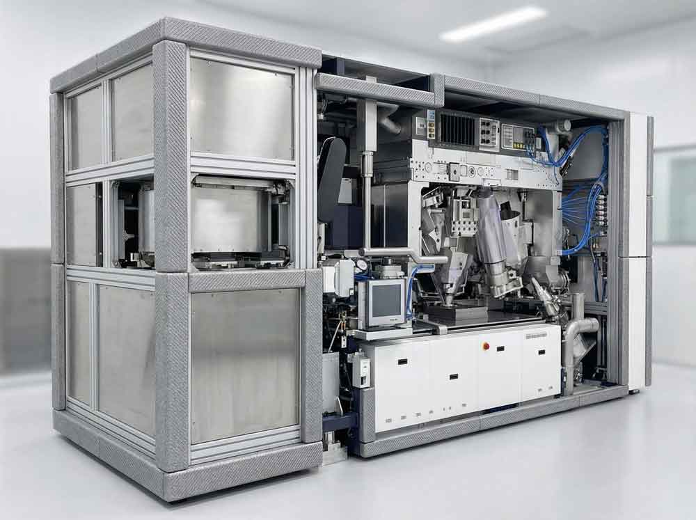
a. Challenge: High-value precision equipment vulnerable to impact and energy inefficiency
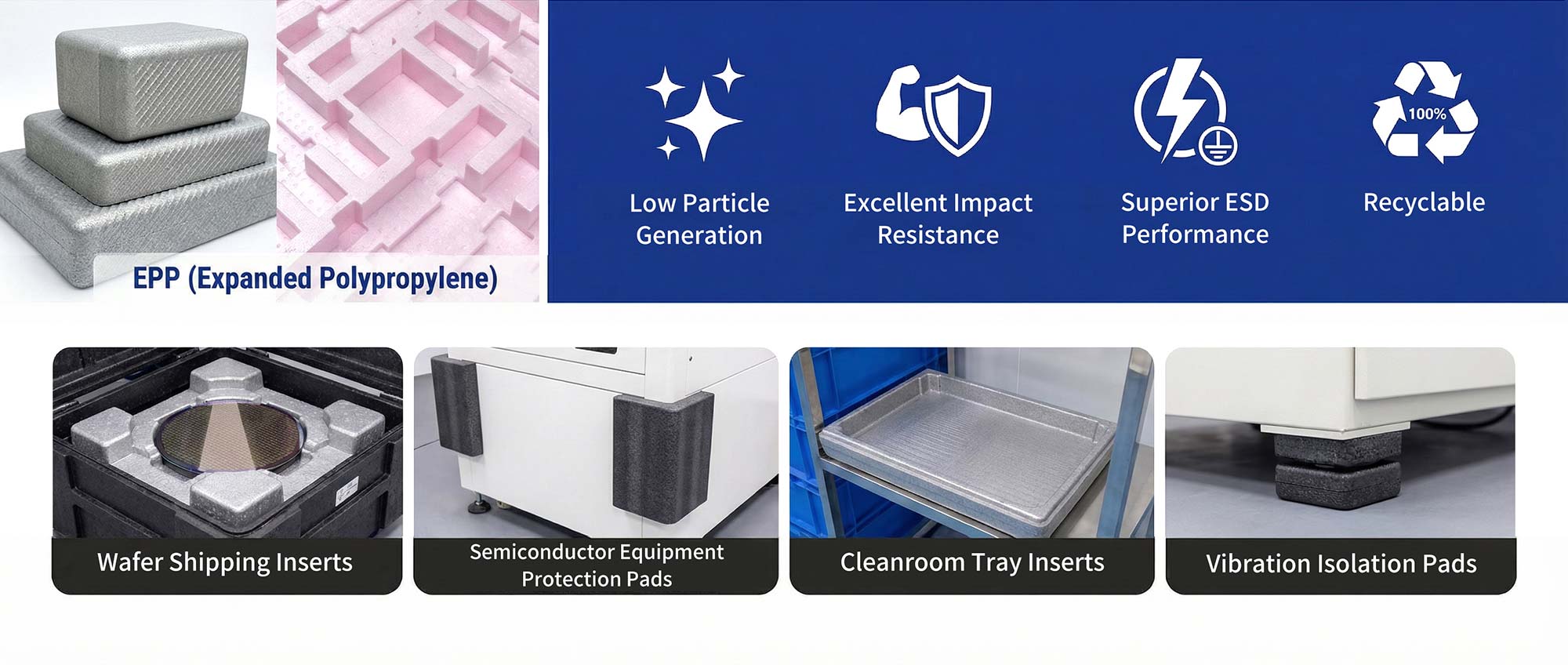
b. Material Selection: Clean-grade EPP + EPO composite system
c. Core Benefits: Impact absorption with dust-free performance; lightweight structural design; reduced energy consumption compared with metal components
d. Applications: Lithography machine housings, etching equipment edge protection, and inspection equipment enclosures
e. Image: EPP impact protection on lithography equipment
Precision Vibration & Positioning Control
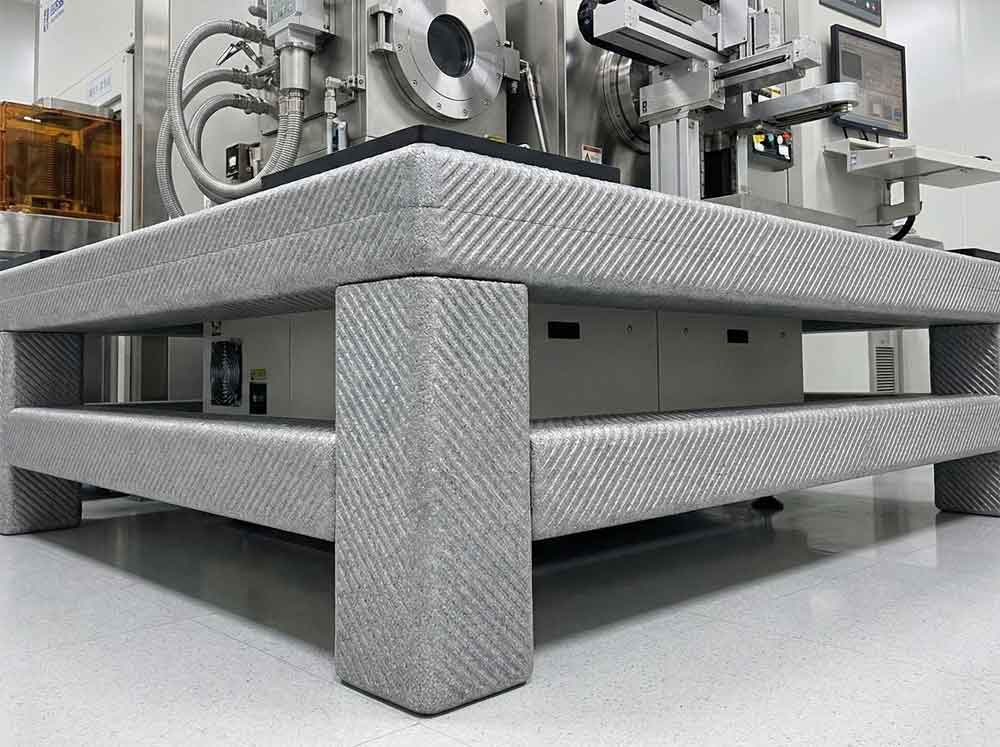
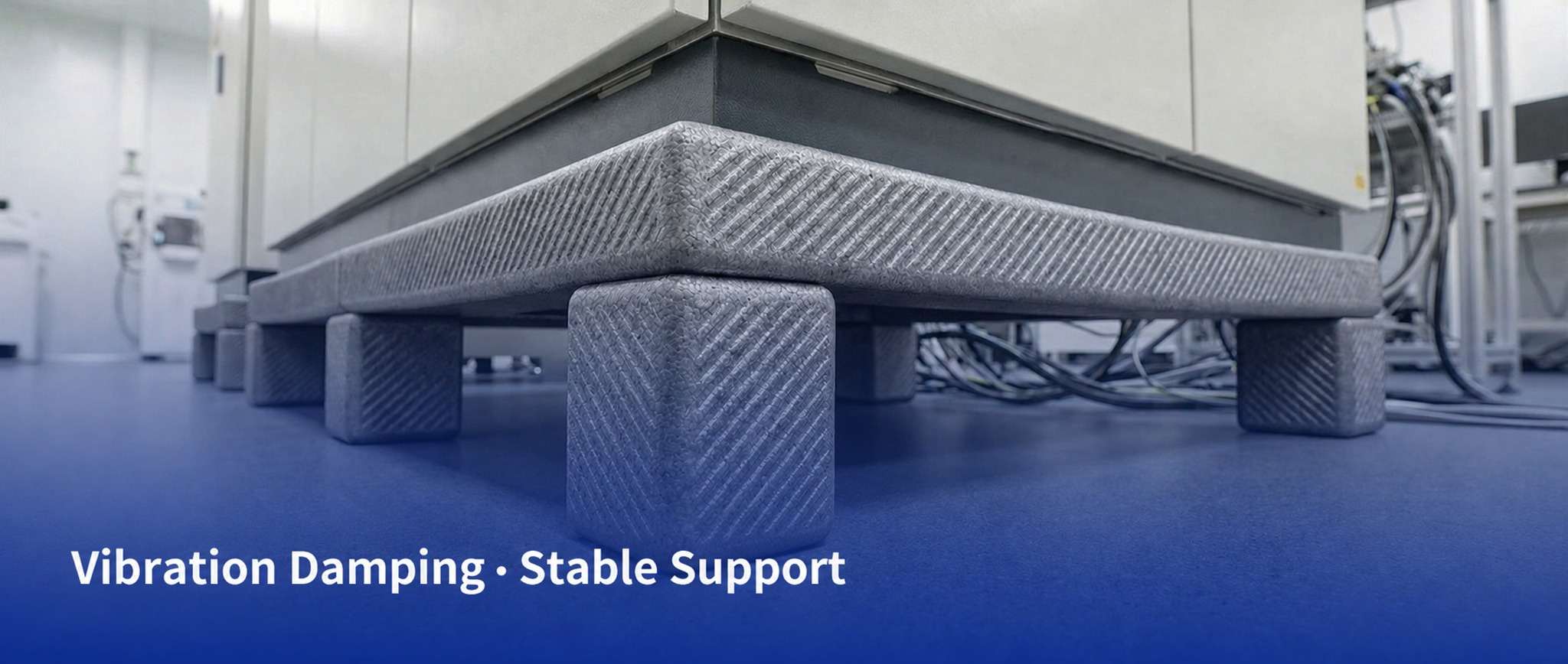
a. Challenge: Process vibration reduces precision and causes alignment deviation
b. Material Selection: High-resilience EPP
c. Core Benefits: Effective vibration damping; improved process stability; anti-slip and zero displacement performance
d. Applications: Lithography systems, ion implantation tools, and inspection equipment vibration isolation
e. Image: EPP vibration damping foot for semiconductor equipment
2. Semiconductor Equipment Protection
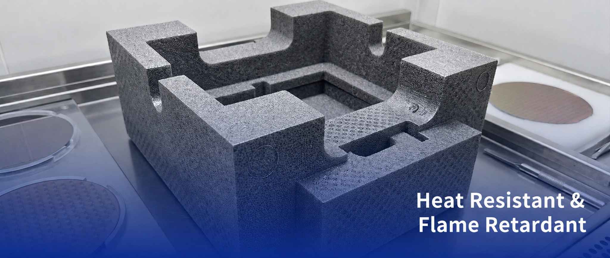
High-Temperature Process Thermal Protection
a. Challenge: High-temperature conduction damage and low-temperature instability
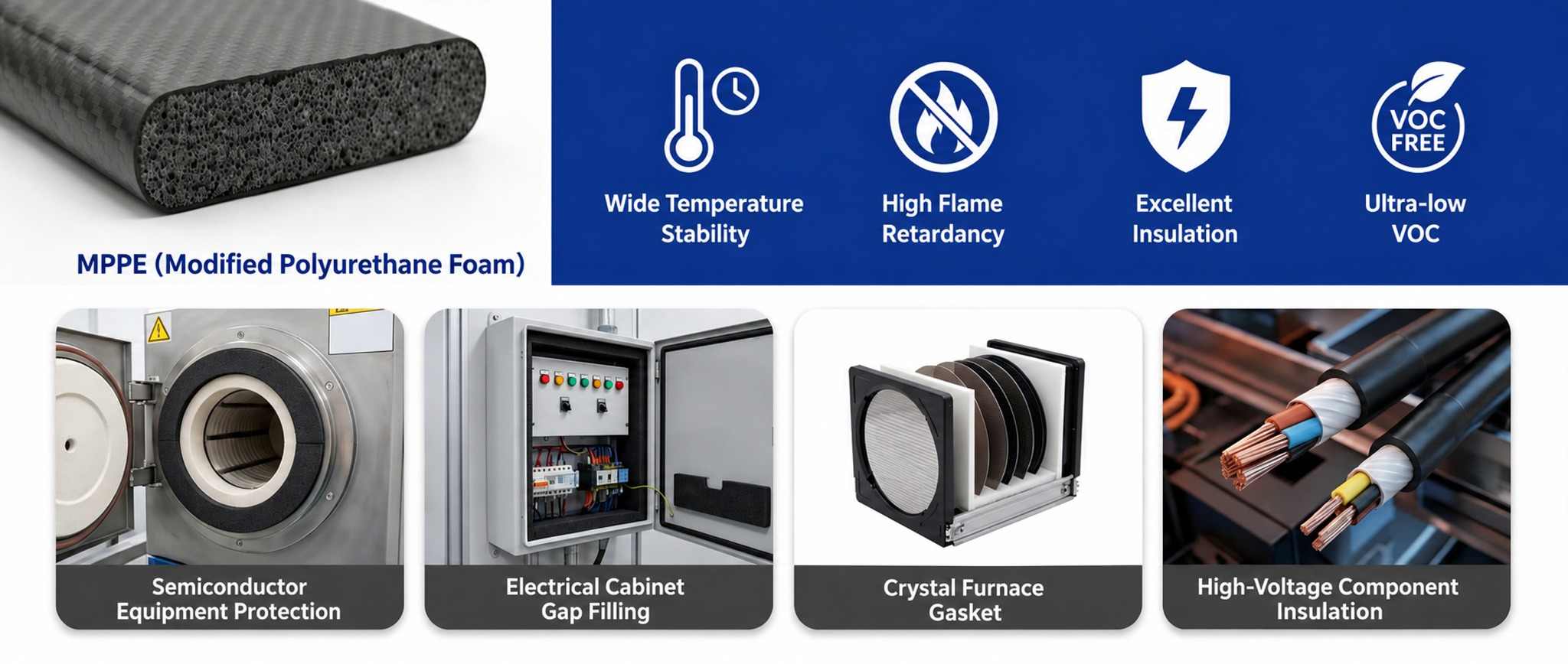
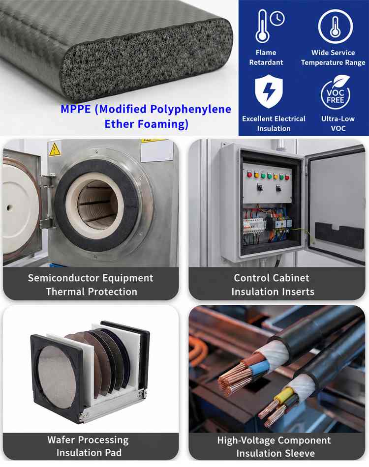
b. Material Selection: Flame-retardant MPPE + EPS insulation layer
c. Core Benefits: MPPE withstands up to 110°C with flame resistance; EPS maintains thermal stability; ensures process precision
d. Applications: Annealing furnaces, low-temperature plasma etching systems, and packaging test thermal zones
e. Image: MPPE protection component in annealing furnace
Packaging test fixture and buffer
a. Challenge: Fixture contamination and probe damage during testing
b. Material Selection: EPO fixture pads + EPE cushioning components
c. Core Benefits: Low-outgassing and chemical resistance; anti-static buffering; prevents probe-induced damage
d. Applications: Chip packaging fixtures, test platform pads, and probe card protection
e. Image: EPO fixture pad for semiconductor testing
3.Process & Packaging Testing Scenarios
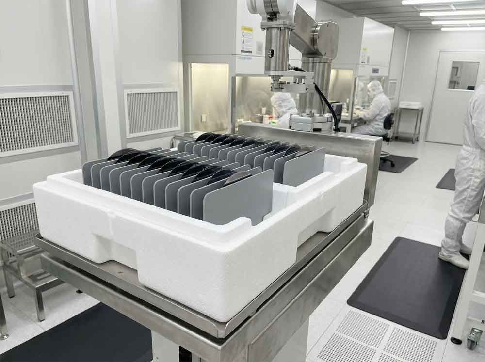
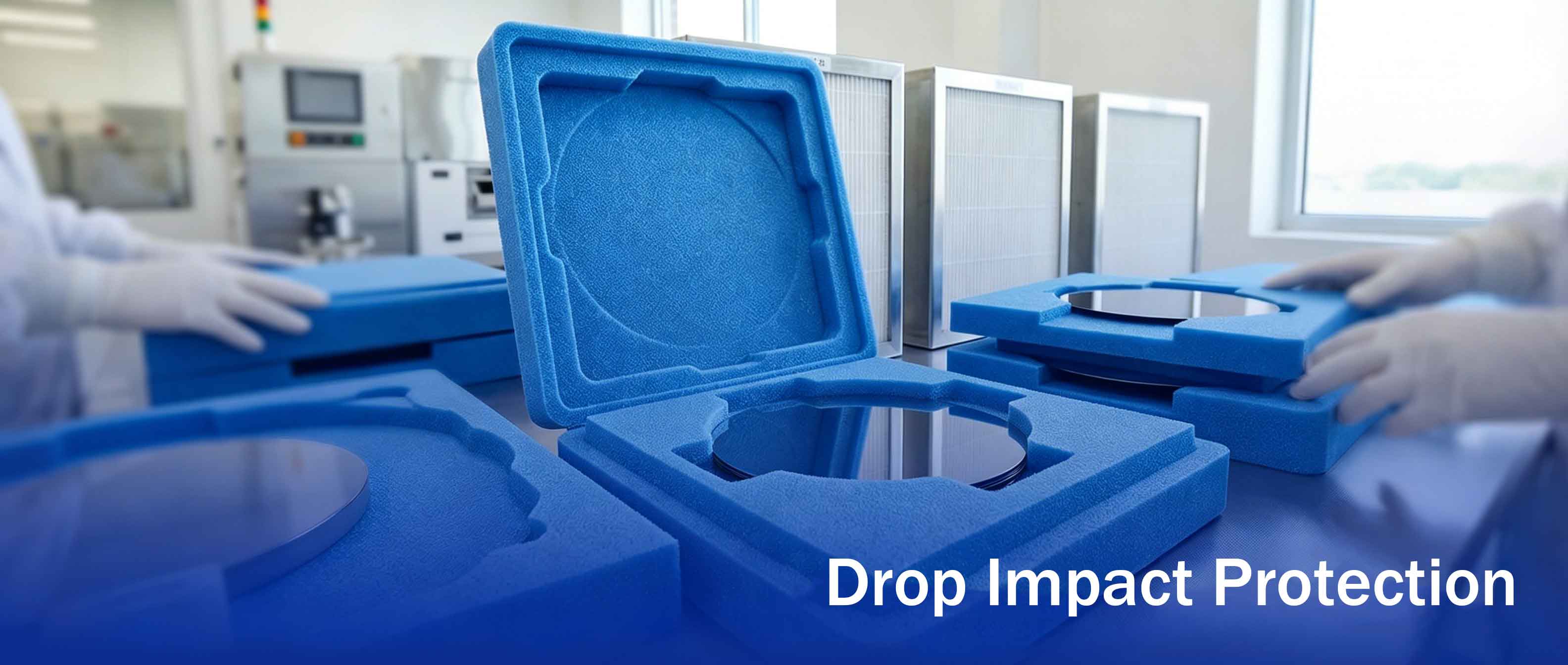
Cleanroom Handling & Storage
a. Challenge: Dust and static contamination during handling in clean environments
b. Material Selection: Clean-grade EPP trays + EPO separators
c. Core Benefits: Dust-free and reusable; anti-static and chemically resistant; compatible with cleanroom protocols
d. Applications: Wafer transfer trays, device storage racks, and robot handling carriers
e. Image: EPP cleanroom transport tray
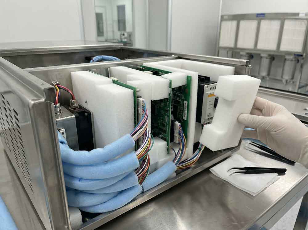
Auxiliary Equipment Protection
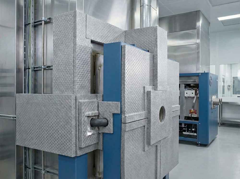
a. Challenge: Electrical short circuits and cable wear causing contamination risks
b. Material Selection: MPPE insulation components + EPE cable protection layers
c. Core Benefits: Excellent insulation and dust-free performance; soft anti-scratch protection; anti-static capability for cleanroom wiring
d. Applications: Cleanroom control cabinets, equipment cabling systems, and vacuum equipment protection
e. Image: MPPE insulation component in control cabinet